
Fudan team invents wafer level silicon based two-dimensional complementary stacked transistor
Recently, according to news on the official website of Fudan University, the Fudan team has invented a wafer level silicon based two-dimensional complementary stacked transistor
Traditional integrated circuit technology uses planar unfolded electronic and hole transistors to form complementary structures, thereby achieving high-performance computing power. The increase in density is mainly achieved by reducing the size of the unit transistor.
For example, industries below 7nm nodes use extreme ultraviolet lithography technology to achieve high-precision size reduction. The complexity of extreme ultraviolet lithography equipment highlights the value of three-dimensional stacked complementary transistor (CFET) technology, which can significantly improve the integration density under existing technological nodes. However, the process complexity of all silicon based CFET is high, and its performance deteriorates severely in complex process environments.
Therefore, the research and development of CFET devices and integrations that are highly compatible with mainstream technologies in China is of great significance for the independent development of new integrated circuit technologies.
In response to this key technology, Professor Zhou Peng from the School of Microelectronics at Fudan University, researcher Bao Wenzhong, and researcher Wan Jing from the School of Information Science and Engineering have innovatively proposed silicon based two-dimensional heterojunction integrated stacked transistors. This technology utilizes mature backend processes to integrate new two-dimensional materials onto silicon based chips, and utilizes the highly matched physical characteristics of the two to successfully achieve a 4-inch large-scale three-dimensional heterojunction integrated complementary field-effect transistor. Under the same process node, the device integration density was doubled and excellent electrical performance was achieved.
It is reported that the research team of Fudan University has introduced a new type of two-dimensional atomic crystal into the traditional silicon based chip manufacturing process, achieving wafer level heterogeneous CFET technology. Compared to silicon materials, the single atomic layer thickness of two-dimensional atomic crystals gives them superior short channel control capabilities in small-scale devices.
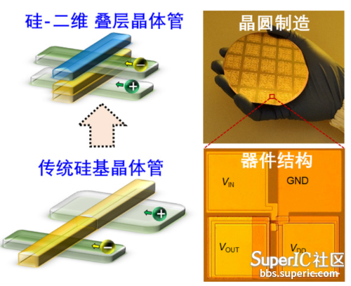
The research team utilized the standard backend process of silicon-based integrated circuits to stack molybdenum disulfide (MoS2) three-dimensional on traditional silicon-based chips, forming a heterogenous complementary CFET structure of p-type silicon-n type molybdenum disulfide. The low-temperature process of molybdenum disulfide is highly compatible with the current backend process of silicon-based integrated circuits, greatly reducing process difficulty and avoiding device degradation. At the same time, the carrier mobility of the two materials is close, and the device performance is perfectly matched, making the performance of heterogeneous CFET superior to traditional silicon based and other materials. The team also verified the application of this new device in "all in one" photoelectric detection and gas sensing.
Currently, larger wafer level heterogeneous CFET technology based on industrial production lines is being developed. This technology will further enhance the integration density of chips, meet the development needs of high computing power processors, high-density memory, and artificial intelligence applications, and help break the technological blockade in the field of large-scale integrated circuits abroad.
Share

